
The Chill of Progress: How Bringing Electronics Closer to Qubits Could Unlock Scalable Quantum Computing
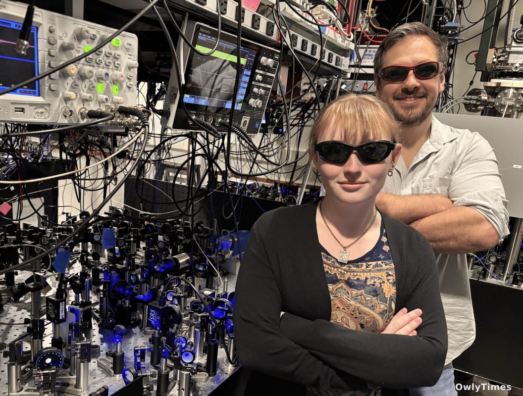
The pursuit of a practical quantum computer isn’t simply about building bigger and faster processors; it’s a fundamental engineering challenge of managing the delicate quantum states – qubits – that underpin the technology. For ion-trap quantum computers, a leading architecture, that challenge increasingly centers on the sheer complexity of controlling a growing number of qubits. Recent work from a collaboration between Fermi National Accelerator Laboratory and MIT Lincoln Laboratory offers a compelling, if preliminary, solution: move the control electronics inside the refrigerator. This isn’t about incremental improvement; it’s a potential paradigm shift in how we approach scaling quantum systems, and the initial results, published as an insider brief and press release, reveal both the promise and the considerable hurdles ahead.
Source material: thequantuminsider.com.
The core problem lies in the current architecture of most ion-trap systems. Qubits are created using individual ions – charged atoms – suspended and controlled by electromagnetic fields. These ions require incredibly precise manipulation, traditionally achieved with lasers and a dense network of wiring connecting room-temperature electronics to the ultra-cold environment where the ions reside. As the number of qubits increases, so does the wiring, creating a bottleneck in terms of space, power consumption, and, critically, thermal noise. This noise, even at minuscule levels, can disrupt the fragile quantum states, leading to errors. The Quantum Science Center, led by Oak Ridge National Laboratory, and the Quantum Systems Accelerator, led by Lawrence Berkeley National Laboratory, recognized this limitation and funded a project to explore integrating control circuits directly into the cryogenic environment. The team, spearheaded by Sandia National Laboratories in collaboration with MIT Lincoln Laboratory, successfully demonstrated that this “in-vacuum cryoelectronics” approach is, in principle, viable.
What the study actually found is not a fully realized quantum processor, but a proof-of-concept. Researchers successfully trapped and manipulated ions using circuits developed at Fermilab and integrated into an existing ion-trap platform at MIT Lincoln Laboratory. They demonstrated the ability to move individual ions, hold them in place, and measure the impact of electronic noise – all crucial functions for quantum computation. This is a significant step beyond simply showing the electronics can survive the extreme cold; it proves they can function within the system. Travis Humble, director of the Quantum Science Center, described the research as integrating “state-of-the-art capabilities in quantum technologies to deliver an exciting new direction for scalable ion trap quantum computing using cryoelectronic control chips.” However, headlines proclaiming a breakthrough in scalable quantum computing should be viewed with caution. The demonstration involved a relatively small number of ions and represents an early stage in a complex development process.
The success isn’t merely about proximity. By placing the electronics closer to the qubits, the team drastically reduced the length of the wires needed, minimizing a major source of thermal noise. Furthermore, the low-power design of the cryoelectronics themselves contributes to a cleaner signal. Farah Fahim, head of Fermilab’s Microelectronics Division, emphasized that demonstrating the feasibility of this approach “may be able to accelerate the timeline for scaling quantum computers, bringing closer into reach what seemed decades away.” But the experiment also revealed unexpected challenges. Transistors that performed well in Fermilab’s testing environment struggled in the even colder temperatures at MIT Lincoln Laboratory, impacting circuit performance. Initial voltage hold times were measured in milliseconds, far short of the minutes or hours required for complex quantum operations.
Engineering Realities and the Limits of Current Designs
These discrepancies highlight a critical tension: the performance of materials and components changes dramatically at cryogenic temperatures. What works in a controlled laboratory setting doesn’t necessarily translate to a real-world quantum computer. The team discovered that the optimal design parameters for transistors shift significantly, requiring a re-evaluation of materials and fabrication techniques. This isn’t a fatal flaw, but it underscores the need for dedicated research into cryo-compatible electronics. The current generation of transistors, designed for room-temperature operation, are simply not optimized for these extreme conditions. Moreover, the limited voltage hold times represent a significant obstacle. Maintaining a stable voltage is essential for precisely controlling the ions, and the current system requires frequent refresh cycles, adding complexity and potential for error. Robert McConnell, a technical staff member at MIT Lincoln Laboratory, acknowledged these challenges, stating that the demonstration “lays the foundation for hybrid-integrated systems we hope to develop in the near future,” but significant work remains.
The collaborative nature of this project is also noteworthy. The expertise of Fermilab in microelectronics development complemented MIT Lincoln Laboratory’s established ion-trap platform, creating a synergy that accelerated progress. This model of cross-center collaboration, facilitated by the Department of Energy’s National Quantum Information Science Research Centers, is likely to become increasingly important as the field matures. Quantum computing isn’t a problem that can be solved by a single institution or discipline; it requires a coordinated effort across multiple areas of expertise. However, the reliance on national laboratory resources also raises questions about accessibility. Will this technology be readily available to researchers outside of these large institutions, or will it remain concentrated within a select few?
What Comes Next: Direct Integration and the Search for Robustness
The next steps are clear: direct integration of the cryoelectronics with the ion-trap chips. Currently, the Fermilab-developed circuits are mounted near the ion trap, but a more tightly coupled design would further reduce wiring and improve performance. This requires developing new fabrication techniques that allow for the seamless integration of different materials and components at cryogenic temperatures. Simultaneously, researchers will focus on improving the voltage hold times and optimizing transistor performance. This will likely involve exploring new materials, such as specialized semiconductors designed for cryo-operation, and developing novel circuit architectures that are less susceptible to noise.
Looking ahead, the critical question isn’t just if we can scale ion-trap quantum computers, but how robust those systems will be. A quantum computer with thousands or even millions of qubits is useless if those qubits are constantly plagued by errors. The success of this in-vacuum cryoelectronics approach hinges on its ability to significantly reduce those errors, not just by minimizing thermal noise, but also by creating a more stable and reliable control system. Will future iterations of this technology demonstrate a measurable improvement in qubit coherence times and gate fidelity? That’s the metric to watch as this promising research continues to unfold.